Search
NEWS

Schematic of channels with (a) non-overlapped electrical double layers

By A Mystery Man Writer

Schematic of channels with (a) non-overlapped electrical double layers

Decentralized Organizational Structure - FourWeekMBA

Schematic of channels with (a) non-overlapped electrical double layers

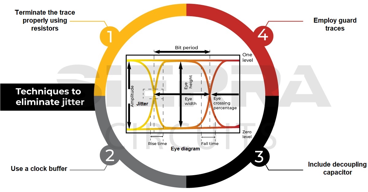
Techniques to Measure and Avoid Jitter in PCBs

Schematic of channels with (a) non-overlapped electrical double layers

PDF) Theory and experiments of concentration polarization and ion focusing at microchannel and nanochannel interfaces

Schematic of channels with (a) non-overlapped electrical double layers

Electrical Double Layer - an overview

Schematic of channels with (a) non-overlapped electrical double layers

ADUM4177 Datasheet and Product Info

Schematic of channels with (a) non-overlapped electrical double layers

What is a Pad in PCB Design and Development

Schematic of channels with (a) non-overlapped electrical double layers

PDF) Theory and experiments of concentration polarization and ion focusing at microchannel and nanochannel interfaces

Schematic of channels with (a) non-overlapped electrical double layers

How to Prepare Samples for Stimulated Raman Scattering (SRS

Schematic of channels with (a) non-overlapped electrical double layers

A schematic diagram showing (left panel) the electrical double