By A Mystery Man Writer
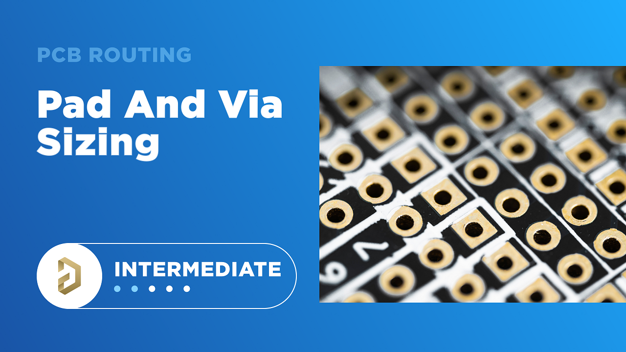
Do you know what PCB via size you should use in your PCB layout? We’ll look at a few simple ways to answer this question.
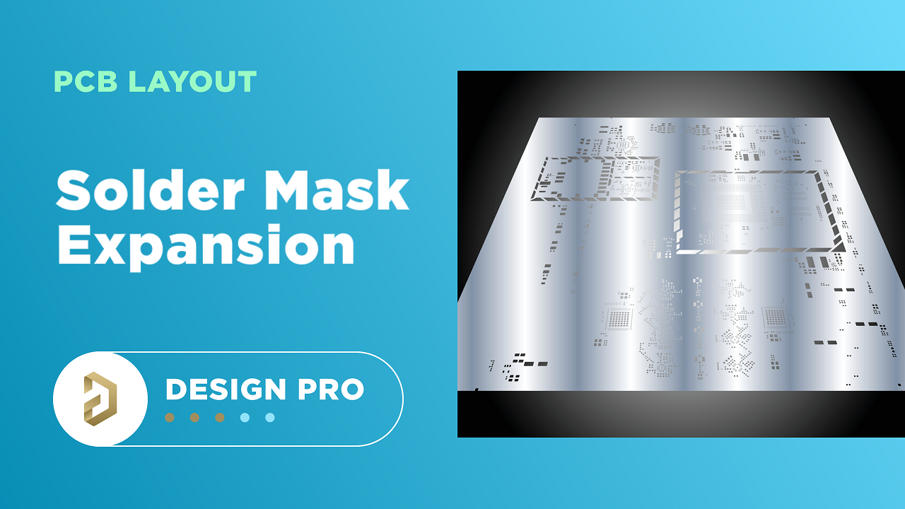
What Solder Mask Expansion Value Should You Use?, Zach Peterson

Review request - ESP32 WROOM module based RS232 controller : r
TECHNICAL PROGRAM - American Chemical Society Publications

Use a PCB Gerber Viewer to Inspect Your Fab Files in Altium 365

The SuperCam Instrument Suite on the NASA Mars 2020 Rover: Body

Seven Days, January 10, 2024 by Seven Days - Issuu

20.000 Most Frequent Words, PDF, Internet

Metal Forming, Fabricating, Welding, & Finishing Buyers Guide by Federal Buyers Guide, inc. - Issuu

Perth092216 by Metroland East - Issuu
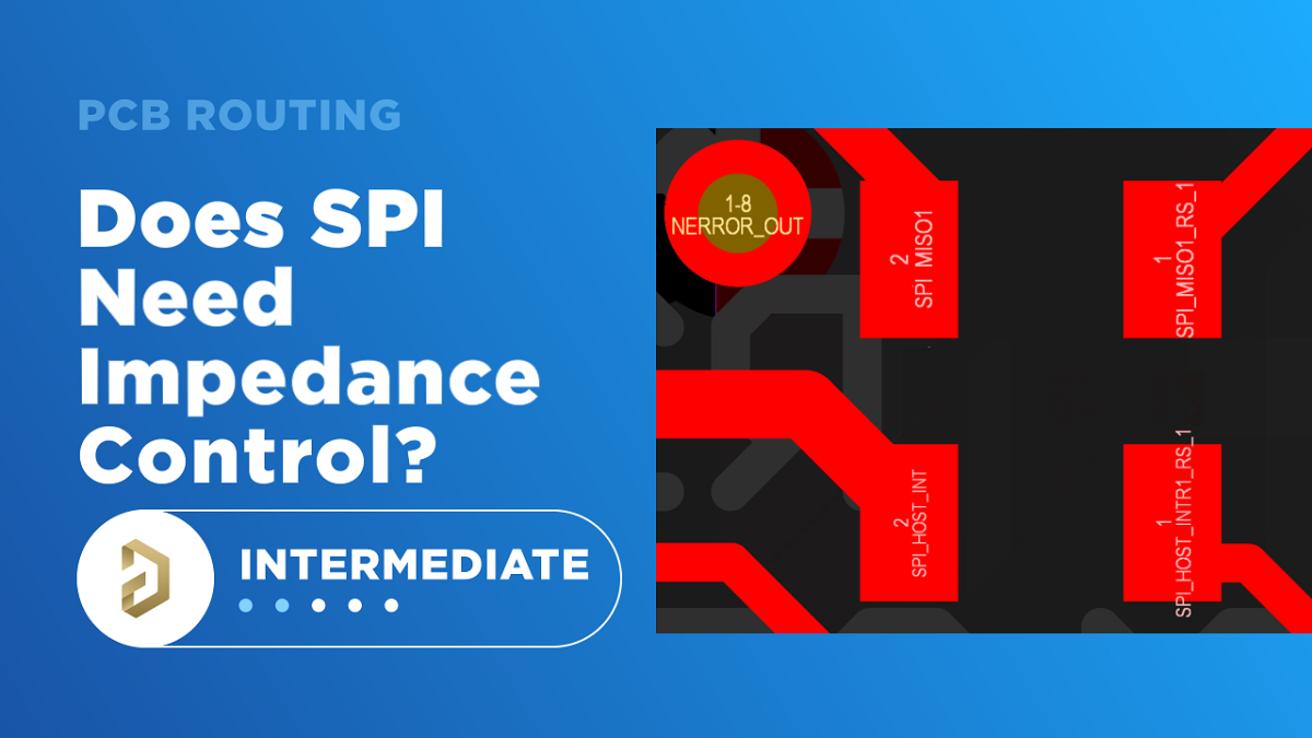
Is There an SPI Trace Impedance Requirement?